




our VISION
Believes that its success is directly tied to the success of its clients, with a firm commitment to the following principles:

Smart and Simple Design
Creating products that are cost-effective and highly reliable.

Professional Service and Dedication
Committing to professional service and complete dedication to all clients

Ease of Assembly and Testing
Designing products for straightforward assembly and testing processes.

24/7 Availability
Ensuring absolute availability for service, support, and guidance throughout the entire project lifecycle, up to the development of the final product.
Excellence, Innovation, and Creativity
Relentlessly pursuing new challenges with a focus on excellence, innovation, and creativity.

Client Success as a Measure of Our Success
The success of our clients' projects is a direct measure of INVIATECH PCB Engineering Ltd.'s success.
About our Company
INVIATECH PCB Engineering Ltd. is a leading company specializing in electronic circuit design from the initial concept to serial production for over 25 years. The company operates with global firms, including Avaya, Intel, Polycom, Sun Disk, defense companies, electronic component development, medical device companies, analog circuits, high-frequency RF circuits, Digital High Speed, 3D Printing, and more. The group is managed by its founder and CEO, Mr. Victor Shimony, who has over 30 years of experience in electronic hardware, circuit design, and process engineering for electrical and electronic systems. The company collaborates and invests significant time and resources in a special program for guidance and consulting for startups.
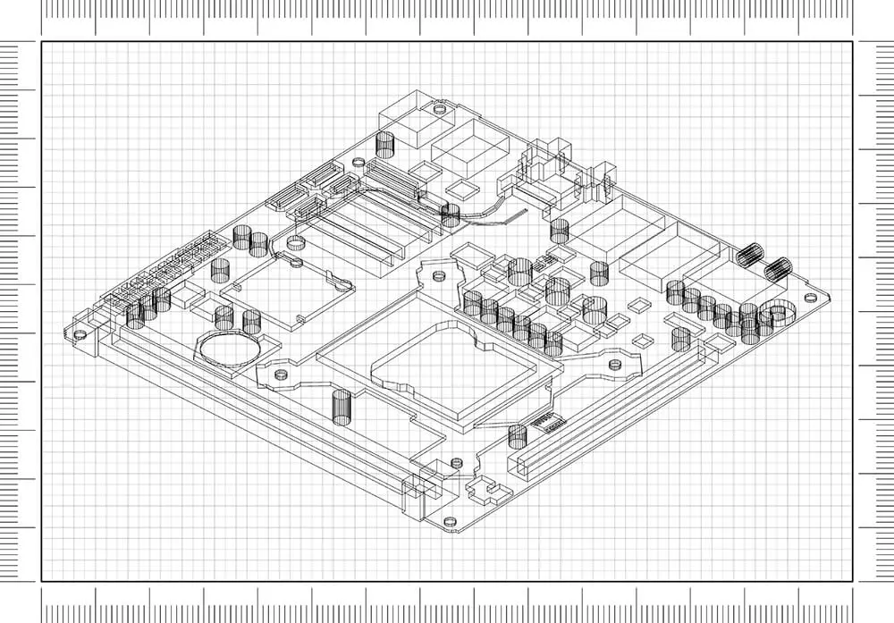
Engineering services for circuit development
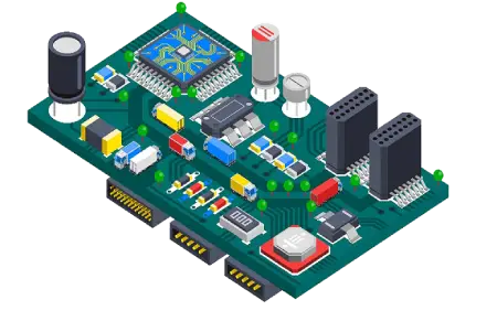
- Analysis of component datasheets
- Considerations for component selection based on the preferred technology for the circuit
- Design considerations for component libraries for electronic schematics, including circuit footprint design
- Mechanical considerations for circuit dimensions in relation to cost, PCB manufacturing, and circuit assembly
- Evaluation of electronic design to meet electrical, thermal, and mechanical requirements, and the PCB manufacturers’ capabilities to provide them at low cost and high reliability
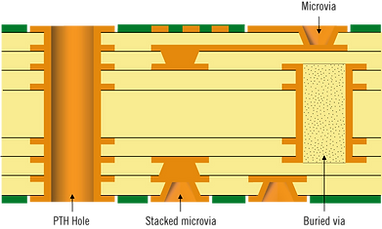
- Component placement and soldering technologies, via connectivity technologies
- Risk assessment and complexity levels, relevant design rules, costs and implications, and decisions
- Layer structure according to the most common and available raw materials for printed circuit board manufacturers, considering the circuit’s electrical requirements, including control impedances, electromagnetic compatibility (RFI, EMI), high-voltage insulation, and more
- On-line editing support for DFM/DFA/DFT/DFC design
- Panel design according to assembly considerations, separation methods, and preparation of DXF files for circuit editing
- Detailed definition of circuit requirements for PCB manufacturers (Class/Solder Finish/Tolerances, coatings and coating thicknesses)
- QA design approval for PCB file release
- Engineering and technological support for PCB manufacturing companies domestically and internationally until PCB production begins
- Support for incoming inspections, engineering quality checks of the PCB before assembly, and evaluation of COC specifications
- Full support of the PCB manufacturing and assembly process, including electrical testing, quality control, packaging, and shipping for development
- Simpler and cheaper PCB manufacturing processes
- High-quality assembly processes with high yield and minimal special effort
- Stable adherence to electrical requirements
- Consistent results in electrical testing within stable limits
- Simple and reduced estimates leading to significant cost savings in product manufacturing
INVIATECH has extensive engineering and technological knowledge and experience, providing a solid foundation for successful circuit revisions in a short cycle and achieving client goals, including Time to Market. Circuit edits are performed using Allegro Cadence software, with potential editing services in additional systems depending on client requirements. Our team includes skilled and professional circuit designers for a wide range of printed circuit boards, including:
- Analog circuits
- High-frequency circuits (RF)
- Back Plane circuits
- High-current and high-voltage circuits
- Integrated Circuit Modules (MCM) – IC Chip Design
- Flexible and rigid-flex circuits
- High-speed digital circuits with experience above 20 GHz
- High-density interconnect (HDI) circuits
What We Need to Provide You with Service:
- Mechanical Drawing – DXF
- Electrical Schematic + Net List
- Bill of Materials (BOM)
- Special Requirements Document for Editing
- Current Requirements by Voltage – Block Diagram, Signal List for Control Impedances
Editing Services Include:
- Guidance and technological consulting for development engineers
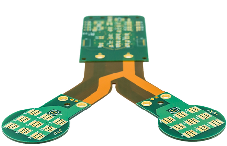 INVIATECH Engineering possesses extensive, proven expertise and experience of over 20 years in printed circuit board (PCB) manufacturing processes. This includes engineering involvement in selecting PCB suppliers, conducting audits for the selection of PCB suppliers across all available raw materials in the PCB industry, evaluating the technological and engineering capabilities of leading PCB manufacturers in China, Europe, and the USA, and designing layer structures based on electrical considerations such as Power Integrity, Control Impedance, and Crosstalk. Our expertise spans a wide range of technologies, including:
- Rigid PCBs
- Flexible PCBs / Multi-FLEX
- Rigid & FLEX PCBs
- Rigid and Flexible PCBs with Ultra HDI technologies
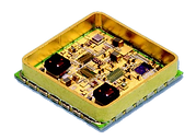
- Miniaturization of circuits, integrating technologies such as Flip Chip, Wire Bonding, and COB (Chip on Board)
- Rigid and Flexible PCBs with hybrid laminations using various materials
- Integrated PCBs with Cavity Heat Sink
- Rigid and Flexible PCBs with multiple laminations (Multi-Lamination)
 Product Support from Development to Production and Assembly
- Product Transition: Support throughout the development phase leading up to production and assembly, including the analysis of circuit documents, system specifications, production files, and special development instructions.
- Technological Support: Providing technical support to manufacturers at all engineering stages, from receiving edited results to the start of PCB production.
- Pre-Assembly Evaluations: Designing paste masks, temperature profiles for Reflow Soldering, and addressing special SMD components such as:
- BGA, Micro-BGA, QFN, Flip Chip, DFN, Power Modules, LGA, POP (Package on Package)
- Assembly Coordination: Coordinating and supervising automated SMT (Surface-Mount Technology) assemblies.
- Soldering Processes: Managing various soldering processes including Vapor Phase, Reflow, Solder Wave, and Selective Wave.
- Special Technologies: Completing assemblies with specialized technologies such as Press Fit connectors, Wire Bonding, and Die Encapsulation.
- Quality Control: Monitoring and inspecting production processes using SPI (Solder Paste Inspection), AOI (Automated Optical Inspection), Microscopes, and X-Ray.
- NPI Report: Writing a professional NPI (New Product Introduction) report.
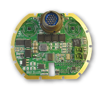
Measurement and Control of Critical Processes in PCB Assembly
Objective: Identify technological and process variables that affect product quality variability to meet required standards, as well as factors impacting the product’s electrical reliability after assembly.
Failure Analysis in Components, PCBs, and Assembly Processes
This area falls under the responsibility of the founder and CEO, Victor Shimoni, with over 30 years of experience.
Victor Shimoni’s decades of proven research on electronic components, printed circuit boards, and electronic assemblies establish him as a high-level professional authority both nationally and internationally. He is adept at identifying failure causes and providing technological solutions for design improvements.
Process Stages
- Story and Description of the Failure: Data Collection
- Product Design Checks (Gerber / CAD / Components Data Sheets) – DFM/DFA
- XRF, 5DX, X-Ray Inspections
- Operating the Product Under Extreme Conditions (ESS) to identify the issue (if the problem is random)
- Laboratory Tests: Metallographic sectioning, chemical tests, EDS/SEM scanning as needed
- Analysis of Results, Drawing Conclusions, and Recommendations for Improvement
Cost Reduction in PCB and PCBA
Reducing costs in PCB (Printed Circuit Board) design and PCBA (Printed Circuit Board Assembly) is essential for boosting profitability and competitiveness. Effective strategies focus on design optimization, material selection, and production efficiency.
PCB Cost Reduction Strategies:
Design Optimization:
- Simplify designs to reduce complexity and layer count.
- Standardize components to lower costs and streamline production.
- Apply Design for Manufacturability (DFM) principles.
Material Selection:
- Choose cost-effective materials and consider bulk purchasing for discounts.
Production Efficiency:
- Optimize PCB layout and minimize drill and routing costs.
PCBA Cost Reduction Strategies:
Assembly Optimization:
- Utilize automated processes to cut labor costs and improve efficiency.
- Reduce rework by designing assemblies to minimize defects.
Component Sourcing:
- Select cost-effective components and negotiate bulk pricing with suppliers.
Process Improvements:
- Enhance yield rates and standardize processes to lower costs and improve efficiency.
Benefits:
- Higher Profit Margins: Reduced production and assembly costs increase profitability.
- Competitive Pricing: Lower costs enable more competitive pricing and market advantage.
- Operational Efficiency: Streamlined processes lead to faster production and improved efficiency.
Implementing these strategies can significantly cut costs while maintaining product quality and performance.
SMT Tooling Development
SMT tooling development involves designing and creating tools for efficient and precise assembly of electronic components on PCBs. Proper tooling enhances manufacturing quality and efficiency.
Key Aspects:
Tool Design:
- Stencil Design: For accurate solder paste application.
- Pick-and-Place Fixtures: For precise component placement.
- Reflow Oven Fixtures: For uniform soldering.
Process Optimization:
- Tool Calibration: Regular checks to ensure accuracy.
- Integration: Ensure compatibility with SMT machines.
Testing and Validation:
- Prototype Testing: Verify tooling performance before production.
- Continuous Improvement: Refine tools based on feedback and data.
Benefits:
- Accuracy: Precise component placement and soldering.
- Efficiency: Faster production and lower costs.
- Reliability: Reduced downtime and maintenance.
Effective SMT tooling is essential for high-quality, efficient surface mount assembly.
SMT (Surface Mount Technology) process engineering focuses on optimizing the manufacturing processes for mounting electronic components onto PCBs (Printed Circuit Boards). This involves designing, implementing, and refining procedures to ensure high-quality, efficient assembly.
Key Areas:
- Process Design: Develop and optimize SMT processes for component placement, soldering, and inspection.
- Equipment Setup: Configure and maintain SMT machinery, including pick-and-place machines and reflow ovens.
- Quality Control: Monitor and adjust processes to ensure high yield and minimal defects.
Benefits:
- Improved Efficiency: Streamlines production and reduces cycle times.
- Enhanced Quality: Ensures consistent, high-quality assemblies.
- Cost Reduction: Minimizes waste and rework.
SMT process engineering is crucial for achieving reliable, high-performance electronics assembly.
Failure analysis involves investigating and diagnosing the causes of failures in electronic components, systems, or assemblies to improve reliability and performance. The process identifies root causes, suggests corrective actions, and helps prevent future issues.
Key Steps:
- Problem Identification: Gather data on the failure symptoms and conditions under which they occurred.
- Root Cause Analysis: Use techniques such as visual inspection, X-ray, and material testing to determine the underlying cause of the failure.
- Corrective Actions: Implement solutions to address the root cause and improve the design, process, or materials to prevent recurrence.
- Documentation and Reporting: Record findings and recommendations to inform stakeholders and guide future improvements.
Benefits:
- Enhanced Reliability: Identifies and mitigates potential issues to prevent future failures.
- Cost Savings: Reduces the need for costly rework and returns by addressing problems early.
- Improved Design: Provides insights for better design and manufacturing practices.
Failure analysis is essential for maintaining high-quality and reliable electronic products by systematically addressing and resolving issues.
Management
The founder and CEO of the company is Victor Shimony. He holds a Bachelor's degree in Electronics and Business Administration from Tel Aviv University, a certified electrical license, a Master's degree in Communication and Management from Tel Aviv University, IPC certification for circuit design, and over 30 years of experience in engineering, manufacturing, and management in the electrical and electronics industry both domestically and internationally.
In 1998, Victor became the Director of Engineering Technologies at Teledata, where he was responsible for hardware product development methodologies, leading engineering efforts, and developing future products for the company. This role included writing procedures, defining engineering processes, circuit edits, and transitioning products from development to production (NPI), including the development and application of advanced PCB technologies for communication circuits, radio circuits, motherboards, and more.
Over the years, Victor has become an expert in various companies in Israel and worldwide regarding technologies and engineering for circuit edits, including DFM/DFA/DFT/DFC design and more.

Additionally, Victor has extensive knowledge and experience in supporting large projects for sophisticated electronics assemblies such as mobile phones, System on Chip (SoC) designs, MCMs, electronic capsules for the medical field, and designing and implementing assemblies for leading companies like Foxconn, Flextronics, Sanmina globally, and many factories in Israel.
Victor also serves as a mentor for advanced PCB technologies in challenging Flex/Flex Rigid circuits, integrating Flip Chip, Wire Bonding, Chip on Board, and utilizing complex HDI technologies. He oversees unique PCB manufacturing and assembly processes while incorporating delicate mechanics in the fields of microelectronics and optoelectronics.
Get in touch
Contact Us:
Feel free to reach out to us via phone, email, or by filling out the contact form below. Our team will respond to your inquiry as promptly as possible. We look forward to hearing from you and exploring how we can assist with your electronic design and manufacturing needs.
Address:
P.O.B 9496, Petah Tikva-4919403


